The Wireless / Wind Logging System for Sourcing ENergy – “Wilssen” is a modular controller for e.g. a wind turbine, it monitors all parameters like phase voltage and efficiency when the wind turbine is generating power.
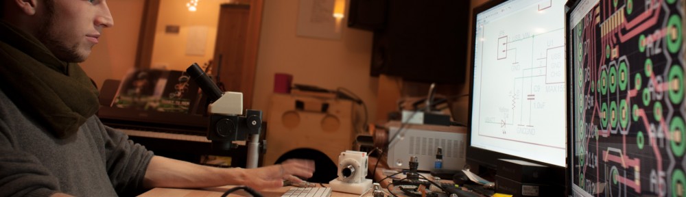
I am working on the first draft of the schematics and the PCB layout. The git repo can be found at GitHub. Wilssen will be compatible with the Optiboot bootloader (read: Arduino compatible) and it features a full breakout of every Arduino pin with the same footprint like the Arduino FIO by Sparkfun, except for the ADC PortPins A0…A7, that particular header is reversed. It’s just a matter of swapping/remapping A0…A7 to A7…A0 in software. The reason for the change are about ten vias which could be eliminated with this simple hack.

It’s definitely impossible to route the board without any vias and without using the bottom layer. However, I am a big fan of single sided SMD layouts and encourage the use of as few vias as possible, because most DIY-folks don’t have the proper tools for vias and they are quite a challenge to master, especially when prototyping at home. I also love the solidity of a printed SMT circuit board without a single hole in it.
The main microcontroller unit can be anything from the Atmel Atmega8 / 168 / 328 family, as long as the pin out is the same. I wired a TQFP footprint in parallel with a tiny MLF package footprint inside. That makes it easy to equip either a larger TQFP or a smaller MLF IC – the latter is more difficult to solder and not recommended for beginners.
All other parts are SMD except for the headers. I won’t populate all of them at my prototypes and most are optional. I think about adding a second footprint for SMD headers on top of the THT-headers, ie make a custom universal footprint.
Resistors and capacitors are mostly 0805 standard size, 1206 are sometimes used as a bridge or via-workaround.
Just like Sparkfun’s Arduino FIO, the Wilssen core controller PCB includes a 1c LiPo charger IC (MAX1555 or MAX1551). The charging circuit is optional to populate and doesn’t take up much space. Great for wireless prototyping on the bench, with the LiPo IC onboard the logic power supply can easily be charged from any USB port.
A0, the analog in 0, the first ADC portpin, is hardwired to a high impedance voltage divider fed directly by the battery voltage and stabilized with a small 100nF cap (any value will do, just for smoothing out the really weak high impedance signal). If the analog reference is set to the internal 1.1V voltage source, the MCU can easily read the current battery voltage and monitor it. A graceful shutdown before the BOD (Brown Out Detection) kicks in should be possible with a periodic check of the battery voltage.
The overall power consumption is minimized and thus there are no power LEDs nor parasitic LEDs at the MOSI/MISO lines. I will include footprints for the typical data and the ordinary power LED, but I don’t recommend to populate them. The current draw of the controller with the attached wireless module in is less than 0.5mA in sleep mode and a single SMD LED will have a huge impact on the battery runtime even if it’s only blinking with a 50% duty cycle. LEDs are fine, but not with the planned inexpensive and tiny 160mAh LiPo cell.
Wiki page with some background info:
http://wiki.opensourceecology.de/wiki/Wilssen
Git repository with up-to-date source code, schematics and issues:
https://github.com/etemu/wilssen
This is of course only a first alpha and heavily WIP, but please feel free to drop me a line if you have any improvements.
- I am still searching for a 4xAA charging IC. I found some expensive ones at National, but those seem too sophisticated and… expensive!

- How should we multiplex the phase voltage and current measurements? Analog multiplexing IC after the Amplifier stage or before?
- Should there be OpAmps onboard with configurable gain through jumpers or unpopulated pads or should those also be outsourced to the e.g. current sensor boards
 .
.


Are you published this also elsewhere? There are maker many communities for PCB design which could help out and connect to OSE. Some additional links, for instance to http://wiki.opensourceecology.de/wiki/Wind_Turbine could also help to direct readers of this blog article to the right sources and documents.
Thanks Jakob, I added links to the wiki entry and the repository at GitHub.
Yes, if we post it somewhere in good electronics forums it could lead some of their experts to support us?
Good work, btw. Very promising! 🙂